
At 2:18 p.m. on November 7, 2019, the completion and operation of etch cleaning project of Shanghai (Ferrotec) Intelligent Technology Development Co., Ltd. and the Establishment Ceremony of cleaning and testing center were held as scheduled.

The main leaders and guests attending the completion and production ceremony are:
Mr. He Xianhan, deputy president of the suppression service, chairman of the board of directors of Ferrotec China and chairman of Shanghai(Ferrotec)Intelligent Technology Development Co., Ltd. of Japan Magnetic Technology Holding Co., Ltd;
Mr. Yamamura, deputy president of Japan Magnetic Technology Holding Co., Ltd;
President of Japan Magnetic Technology Co., Ltd;
Gong yongyingzhi, CEO of American Magnetic Technology Co., Ltd;
Guo Jianyue, general manager of Shanghai Shenhe thermomagnetic Electronics Co., Ltd;
Wang Zhe, Ferrotec(Anhui) Technology Co., Ltd. and general manager of Shanghai (Ferrotec)Intelligent Technology Development Co., Ltd.
Also invited to attend today's completion ceremony are semiconductor industry customer representatives, relevant leaders and staff representatives of Ferrotec group.

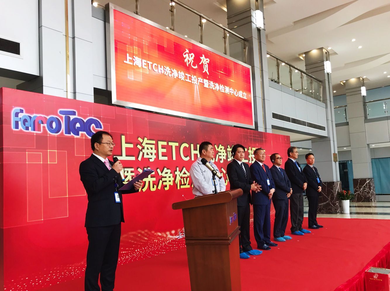
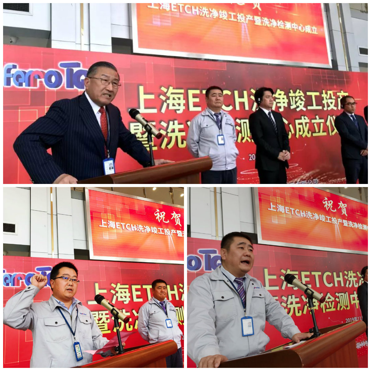
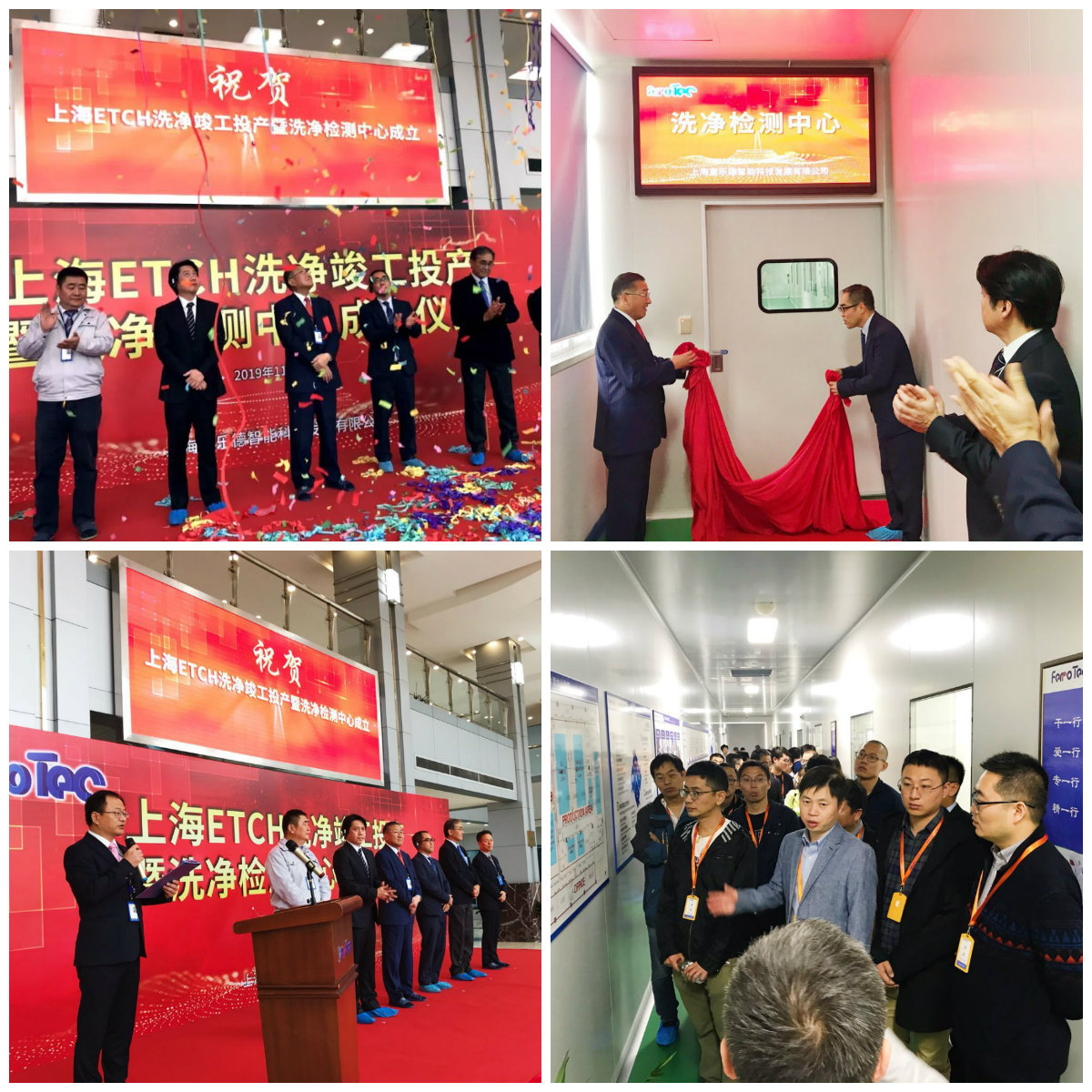
Wang Zhe, general manager of Shanghai (Ferrotec) Intelligent Technology Development Co., Ltd., first introduced the completion and operation of the etch cleaning project and the establishment of the cleaning and testing center. Wang Chengming, the representative of the staff of Shanghai (Ferrotec) etch cleaning project, spoke on behalf of all the staff and made an oath of determination. Mr. He Xianhan, vice chairman of anti service and chairman of Ferrotec China board of directors, delivered a speech on behalf of Japan Magnetic Technology Holding Co., Ltd.

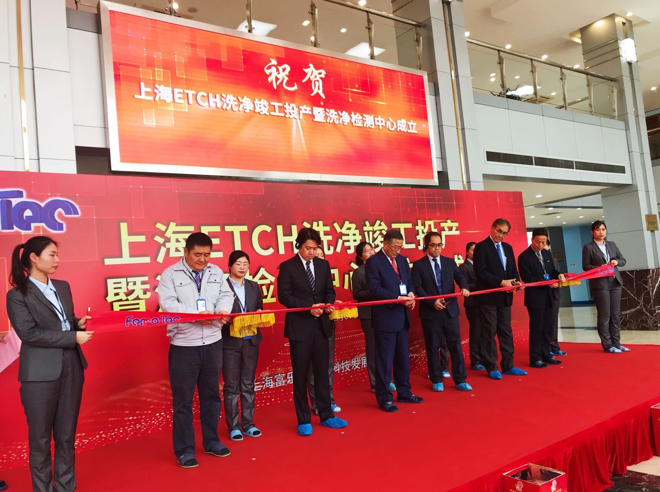
The leaders of the rostrum cut ribbon for the completion and operation of Shanghai etch cleaning and cleaning testing center of Shanghai (Ferrotec)Intelligent Technology Development Co., Ltd., which pushed the ceremony to a climax. Later, general manager Wang Zhe accompanied the group leaders and guests to visit the cleaning and testing center, chairman he Xianhan and vice president of shancunzhang opened the cleaning and testing center and accompanied the guests to visit the etch cleaning and R & D center.

Project Introduction
Shanghai (Ferrotec)Intelligent Technology Development Co., Ltd. is invested by Ferrotec (Anhui)Technology Co., Ltd. the company has been in operation for 5 months since its construction in June 2019. At present, two advanced process etch cleaning production lines and semiconductor detection and Analysis Center have been built.
The company adopts the international leading semiconductor component surface treatment technology, focusing on the cleaning and renovation of high-level process etching components. In 2020, the introduction of the cleaning technology of the etch parts in the 10 nm process will be completed. No matter in hardware or software system, including production line layout, micro pollution control, measurement data automation, etc., etc., the advanced process etch cleaning production line has been upgraded comprehensively. All products are operated in the 100 level clean room, sampling in the 10 level clean space, and quantitative residue analysis of PPT level has been completed to meet the cleaning requirements of etch devices of 10nm and below The industrial upgrading will greatly improve the reliability and stability of cleaning products, and ensure the leading position of Shanghai fule Intelligent Technology Development Co., Ltd. in the field of professional semiconductor cleaning technology.
Shanghai (Ferrotec) cleaning, testing and Analysis Center will be the first National Key Laboratory of semiconductor testing and analysis with high specification, high standard and high capability, aiming to fill the gap of China's comprehensive testing laboratory in the field of micro pollution quantitative analysis. At the same time, it will become the first testing institution certified by the top three semiconductor equipment manufacturers in China.
Shanghai (Ferrotec) laboratory has precision analysis and detection equipment such as inductively coupled plasma mass spectrometer, ion chromatography, gas chromatography, scanning electron microscope, 3D laser microscope and energy spectrometer, full-automatic potential titrator, Fourier transform infrared spectrometer, thermal desorption gas chromatography / mass spectrometry. It can provide services of morphology characterization and micro pollution quantitative analysis and detection. For example, quantitative analysis of elements and ions in water / gas, analysis and detection of metal pollution, chemical residue, organic pollution and particle pollution on the surface of components, etc.; meanwhile, the laboratory will also undertake the analysis and guarantee work during the development of new products and processes, and escort the stability and reliability of high-level process cleaning processes to meet the growing high-end semiconductor industry Clean up the market demand.