

Nowadays, the localization of semiconductor chips has been promoted to the level of national strategy. In the face of this situation, how can silicon wafer, as the core basic material of integrated circuits, exert its power? On the morning of November 22, the completion and production ceremony of the semiconductor wafer project of Hangzhou semiconductor Wafer Co., Ltd.(FTHW) was ceremoniously held in the outdoor square of the administrative building of the plant area, which is another significant leap forward in the strategic layout of the semiconductor industry of Ferrotec (China) group, and can effectively alleviate the shortage of large-scale silicon wafer materials in China.

At 10:28 a.m. on November 22, the completion and production ceremony of the semiconductor wafer project of Ferrotec (China) Group FTHW was held! This marks that the semiconductor wafer project has officially entered a new stage from construction to trial production to mass production. Ferrotec (China) group has gradually formed a Ferrotec wafer industry cluster integrating Hangzhou factory (200 mm, 300 mm silicon wafer processing), Shanghai factory (200 mm, 150 mm silicon wafer processing) and Yinchuan factory (silver and semiconductor: single crystal long crystal) The domestic and foreign markets provide the real mass production of large semiconductor silicon chip with independent core technology!
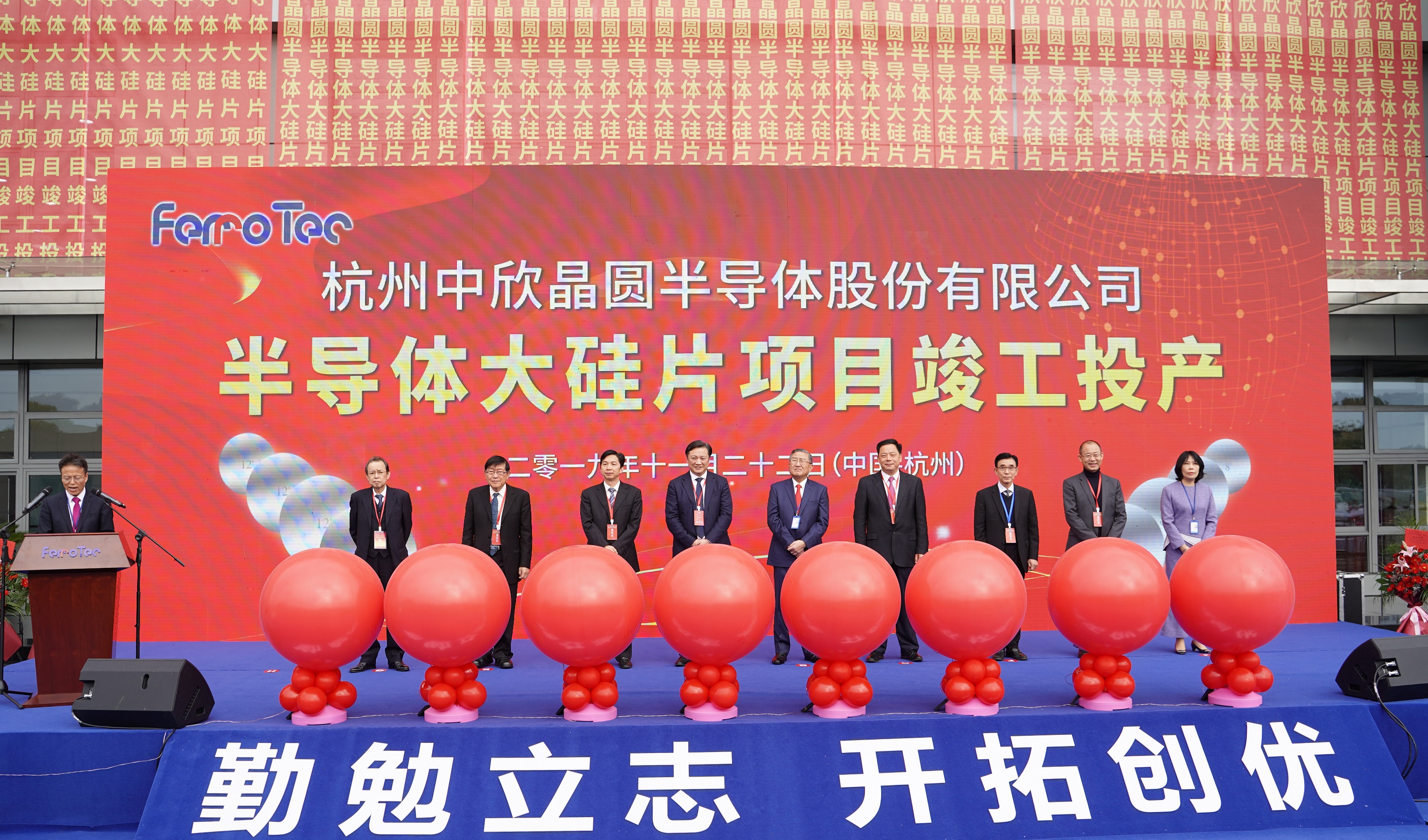
The completion and production ceremony has aroused great repercussions in the semiconductor industry, attracting guests from all walks of life at home and abroad to attend and give congratulations. The ceremony was attended by Mr. Hu Wei, vice mayor of Hangzhou Municipal People's government, Mr. He Meihua, director of Hangzhou Qiantang New Area Management Committee, Mr. Xia Jiliang, director of Hangzhou Municipal Bureau of economy and information technology, Dr. Zhang Rujing, chairman of Xinen (Qingdao) integrated circuit Co., Ltd., Dr. Yin Zhiyao, CEO of China micro semiconductor equipment (Shanghai) Co., Ltd., and Dr. Zhongxin international integrated circuit manufacturing (Shanghai) Dr. Zhao Haijun, CEO of the limited company, Mr. He Xianhan, deputy president of Ferrotec Holding Co., Ltd., chairman of Ferrotec China board of directors, chairman of FTHW, Mr. Ruo muqinan, vice chairman of FTHW, Mr. Guo Jianyue, director of FTHW and Ms. Dong Xiaoping, director of FTHW. Today's activities are also attended by customers and partners from home and abroad, as well as leaders of Yinchuan City, Ningxia Hui Autonomous Region, Tongling City, Anhui Province, Dongtai City, Jiangsu Province, as well as representatives of relevant employees of various departments of the company.
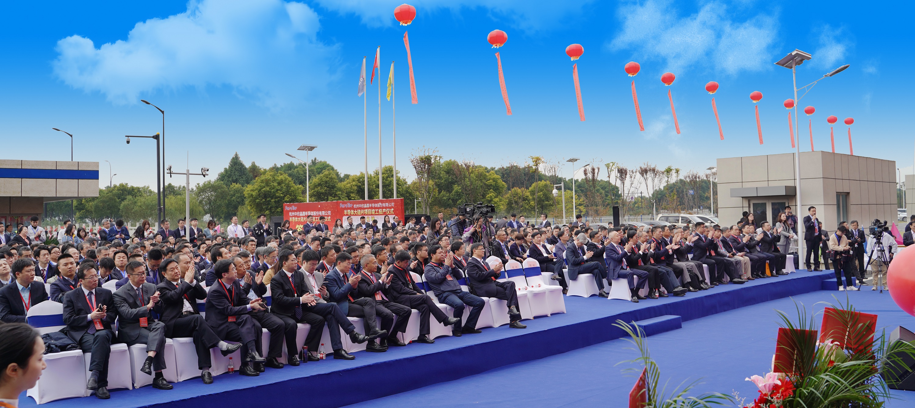
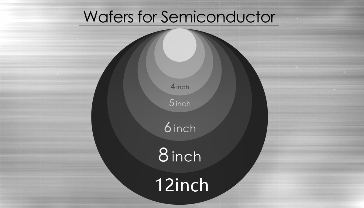
At the beginning of the ceremony, Guo Jianyue, vice chairman of FTHW, introduced the semiconductor large-scale silicon wafer project. On September 28, 2017, Ferrotec (China) Group officially established Hangzhou semiconductor wafer Co., Ltd. in Qiantang new area, Zhejiang Province, with a registered capital of 2.9 billion yuan, covering an area of 133400 square meters and a factory area of 150000 square meters, on the basis of an annual output of 4.8 million 150 million 150 mm semiconductor wafers and 1.2 million 200 mm semiconductor wafers. With a total investment of 6 billion yuan, the project was started on December 18, 2017, which is a major project of integrated circuit industry group in Zhejiang Province. The project has three 8-inch (200 mm) and two 12 inch (300 mm) semiconductor wafer production lines, of which 200 mm production line is the largest and most mature production line in China at present; 300 mm production line is the first semiconductor wafer production line with core technology in China, which can realize mass production. At the end of June this year, the first batch of 200 mm semiconductor large silicon wafers were successfully put off the production line. Now, 300 mm silicon wafers are being debugged. By the end of December, 300 mm silicon wafers will be produced. After mass production, the enterprise can achieve an annual output of 4.2 million 8-inch semiconductor wafers and 2.4 million 12 inch semiconductor wafers.
Guo Jianyue also introduced that the products of Zhongxin wafer project have the advantages of high flatness and strong stability, and the silicon produced will mainly be supplied to the domestic market. The company is committed to becoming a benchmark base enterprise for the production of China's semiconductor large silicon wafers and one of the major suppliers of semiconductor silicon polishing wafers in the world.
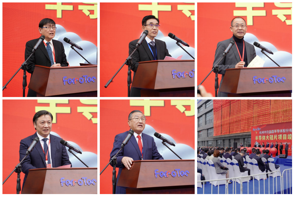
Later, in the speech stage, the industry experts and municipal government leaders expressed their confidence in the rise and rapid development of China's semiconductor integrated circuit industry, and the determination of Hangzhou municipal / district government to vigorously support and support the semiconductor industry.
Dr. Zhang Rujing, Dr. Yin Zhiyao and Dr. Zhao Haijun all said that China has become the most important market for the global integrated circuit industry. Under the background of national strategic support, the development of China's integrated circuit industry can not be separated from the concerted efforts of all walks of life in the industrial chain to jointly build an integrated industrial ecology and realize the ecological sharing, standard co construction and channel between the two sides We will work together to promote the prosperity and development of the industry. At the same time, the development of the industry is closely related to the support of the government. Vice Mayor Hu Wei said that it is the result of our joint efforts to add new energy levels to the intelligent manufacturing industry in Qiantang new area. The launch of the Zhongxin wafer project is highly consistent with Hangzhou's strategy to fully promote the integrated circuit industry. Hangzhou municipal / district government will continue to vigorously support and closely cooperate with Zhongxin crystal The development of the circle will contribute to the development of the IC industry in Hangzhou, and further improve the cooperation mechanism and industrial structure between the IC design enterprises and the material / equipment manufacturing industry!
Today's completion ceremony also received congratulations from all parties. Dr. Zhang Rujing, chairman of Sinn (Qingdao) integrated circuit Co., Ltd., presented congratulations to Mr. He Xianhan, chairman of Ferrotec Holdings Co., Ltd., Mr. ruoku Qinan, to Mr. Guo Jianyue, and together with Mr. Tai Jiabin, pressed the fingerprint on the screen as the large silicon project of FTHW Production assistance.


After the ceremony, accompanied by chairman he Xianhan and others, the guests visited the 8-inch and 12 inch semiconductor wafer production lines. President he once again introduced the strategic layout and future development plan of the project to the guests in detail, and focused on the scale of production line, maturity and innovation of production line technology.
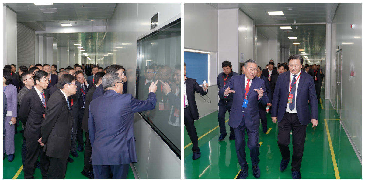
The integrated circuit industry is a national pillar industry. The successful completion and operation of Hangzhou Zhongxin wafer semiconductor large-scale silicon project has accelerated the strategic layout process of China's integrated circuit industry. FTHW will also aspire to become a benchmark factory for the production of China's semiconductor large-scale silicon wafer, with continuous and rigorous on-site management and continuous promotion of "standardization, visualization, digitization and self Moving, improving production efficiency, filling the gap of large-scale production of large-diameter silicon wafers in China, breaking the long-term monopoly of foreign companies on the semiconductor silicon wafer market, and realizing the real "made in China" in the semiconductor silicon material industry will open a new chapter in the cause of large-diameter silicon wafers in China!