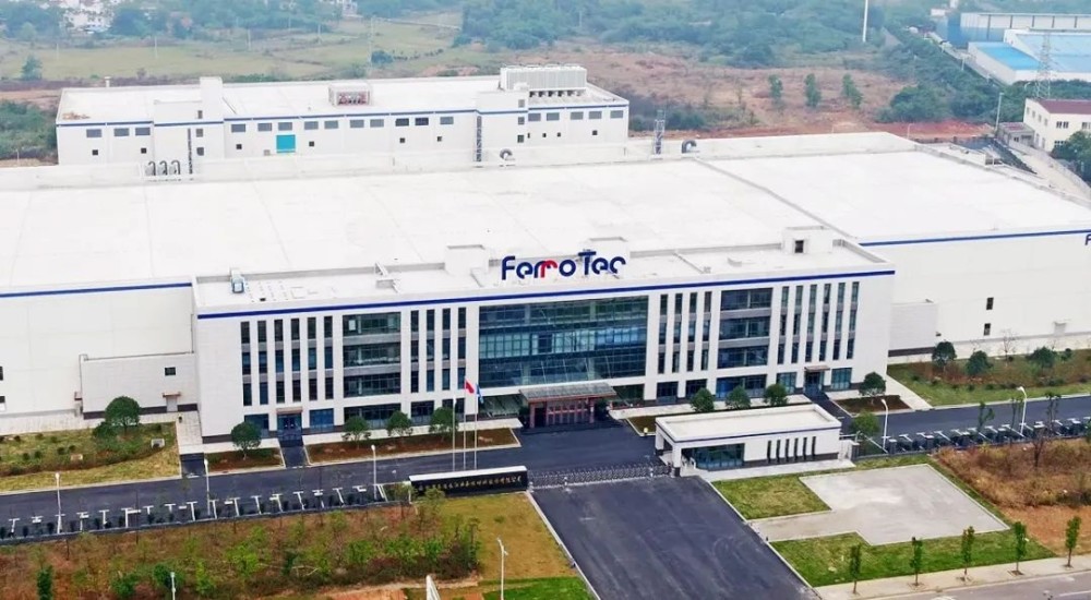

According to Zhongxin wafer, Ferrotec (Anhui) Changjiang Semiconductor Material Co., Ltd., a subsidiary of Ferrotec (China), has invested in the construction of a regeneration project with an annual output of 2.4 million semiconductor wafers. The total investment of the project is planned to be 1 billion yuan, covering an area of 75 Mu and a new factory building of 56774.38 square meters.

It is reported that the project has purchased hundreds of sets of advanced equipment at home and abroad (imported equipment and special equipment are used for key processes), and the construction period is 15 months. After the completion of the project, a production line with an annual output of 2.4 million 300 mm semiconductor wafers will be formed, which can reach the world's advanced level.
IT home learned that, according to the official introduction, Ferrotec (Anhui) Changjiang Semiconductor Material Co., Ltd. was founded in Tongling in 2019 by Shanghai Shenhe Thermo-Magnetics Electronics Co.,Ltd., a wholly-owned subsidiary of Ferrotec Co., Ltd. (Japan Magnetic Fluid Technology Holding Co., Ltd.) in China. Ferrotec Co., Ltd. of Japan formally entered the Chinese market in 1992. Ferrotec (China) has grown into a diversified enterprise group integrating product R & D, manufacturing and sales. It manages more than 20 companies and manufacturing bases all over China, providing world-class materials, devices, equipment and system solutions for customers at home and abroad.
The project is equipped with the most complete wafer recycling production line in China, and is also the first professional manufacturer specializing in the regeneration of 300 mm large-size silicon wafer in China, filling the gap in this field in China. The construction of this project will make the domestic wafer factories get rid of the dilemma of relying mainly on imports for a long time, so that they can achieve high-level large-size wafer regeneration in China.
It adopts the world-class full-automatic precision CMP grinder for 300 mm wafer, which can realize the whole process automation and reduce the thickness loss; the HEPA (high efficiency particulate air) filter device is used inside the equipment to maintain the high cleanliness; in addition, the KLA Tencor SP5 particle detector is used in the measurement equipment, The patternless wafer surface detection system with DUV sensitivity and high throughput, processing and measuring equipment are at the leading level in the international industry.
In the process of project construction, relying on Ferrotec (China) mature semiconductor wafer technology talent team as the foundation, foreign expert team directly participates in equipment procurement, installation and commissioning, and domestic and foreign well-known manufacturers participate in equipment handling and secondary distribution project, with high quality control in each link.